


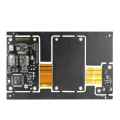
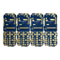
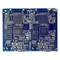
10-layer HDI PCB Board with Material of Rogers
Basic Info
Model No.: hdi flex pcb
Product Description
What is HDI technology?
In addition to smart phones, tablet and desktop manufacturers are striving to achieve miniaturization. All these size reductions depend on the design and use of high-density interconnect PCBs (HDI PCBs). If you think that HDI PCB is only used in smart devices, you are definitely wrong. The functions of HDI technology are designed to make smart devices lighter, smaller, thinner, and more reliable.
HDI PCB refers to high-density, fine-grain, small drill diameter and ultra-thin printed circuit boards. This kind of PCB has developed rapidly on the basis of emerging advantages:
1. HDI technology helps low cost pcb manufacturing;
2. HDI technology increases linear density;
3. HDI technology facilitates the use of advanced packaging;
4. HDI technology has better electrical performance and signal effectiveness (such as High frequency board);
5. HDI technology has better reliability;
6. HDI technology is better in terms of heat dissipation;
7. HDI technology can improve RFI (radio frequency interference) / EMI (electromagnetic interference) / ESD (electrostatic discharge) such as Microwave radio frequency board;
8. HDI technology improves design efficiency;

Some new requirements are put forward for HDI PCB materials, including better dimensional stability, antistatic mobility and non-adhesives. The typical material of HDI PCB is RCC (Resin Coated Copper). There are three types of RCC, namely polyimide metallized film, pure polyimide film, and cast polyimide film.
The advantages of RCC include: small thickness, light weight, flexibility and flammability, compatibility characteristic impedance and excellent dimensional stability. In the HDI multi-layer PCB process, instead of traditional adhesive sheets and copper foil as the insulating medium and conductive layer, the originality electronics IC can be used to suppress RCC through the traditional suppression technology. Non-mechanical drilling methods such as lasers are then used to form micro-via interconnections.
RCC promotes PCB products from Surface-Mount (SMT) & BGA Assembly, from mechanical drilling to laser drilling, and promotes the development and progress of PCB micro-vias, all of which have become RCC's leading HDI PCB materials.
In the actual PCB manufacturing process, for the choice of RCC, there are usually FR-4 standard Tg 140C, FR-4 high Tg 170C and FR-4 and Rogers combined lamination, which are mostly used now. With the development of HDI technology, HDI PCB materials must meet more requirements. Therefore, the main trends of HDI PCB materials should be:
1. The development and application of flexible materials without adhesives;
2. The thickness of the dielectric layer is small, and the deviation is small;
3. The development of LPIC; 4. The dielectric constant is getting smaller and smaller;
5. The dielectric loss is getting smaller and smaller;
6. High welding stability;
7. Strictly compatible with CTE (Coefficient of Thermal Expansion);

The difficulty of HDI PCB manufacturing lies in the microscopic manufacturing, metallization and thin wires.
1. Micro-via manufacturing
Micro-via manufacturing has always been the core issue of HDI PCB manufacturing. There are two main drilling methods:
A. For ordinary through-hole drilling, mechanical drilling is always the best choice for its high efficiency and low cost. With the development of machining capabilities, its application in micro-vias is also constantly developing.
B. There are two types of laser drilling: photothermal ablation and photochemical ablation. The former refers to a process in which the operating material is heated to melt and evaporate through the formed through hole after the high-energy laser is absorbed. The latter refers to the result of high-energy photons and lasers exceeding 400nm in the ultraviolet region.
There are three types of laser systems applied to flexible and rigid boards, namely excimer lasers, ultraviolet laser drilling, and CO 2 lasers. Laser technology is not only suitable for drilling, but also for cutting and forming. Even some manufacturers use lasers to manufacture HDI. Although the cost of laser drilling equipment is high, they have higher accuracy, stable craftsmanship and mature technology. The advantages of laser technology make it the most commonly used method in blind/buried through hole manufacturing. Today, 99% of HDI micro-vias are obtained by laser drilling.

The biggest difficulty of through-hole metallization is that the plating is difficult to achieve uniformity. For the deep hole electroplating technology of micro-via, in addition to using electroplating solution with high dispersibility, the plating solution on the electroplating device should also be upgraded in time. This can be done through strong mechanical stirring or vibration, ultrasonic stirring, and horizontal spraying. In addition, the humidity of the through-hole wall must be increased before electroplating.
In addition to technological improvements, HDI's through-hole metallization method has also seen major technological improvements: chemical plating additive technology, direct electroplating technology, etc.
3. Thin line
The realization of thin lines includes traditional image transmission and direct laser imaging. The traditional image transfer process is the same as that of ordinary chemical etching to form lines.
For direct laser imaging, no photographic film is needed, and the image is formed directly on the photosensitive film by laser. The ultraviolet wave lamp is used for operation, so that the liquid anticorrosion solution can meet the requirements of high resolution and simple operation. Photographic film is not needed to avoid adverse effects caused by film defects. CAD/CAM can be directly connected to shorten the manufacturing cycle and make it suitable for limited and multiple production. Contact us if you need more details on Hdi Flex Pcb. We are ready to answer your questions on packaging, logistics, certification or any other aspects about Quick Hdi Pcb、Hdi Pcb Manufacturing Process. If these products fail to match your need, please contact us and we would like to provide relevant information.
Product Categories : High Frequency Board > HDI PCB